
Predicting a novel two-dimensional BN material with a wide band gap

 , ...
, ... Abstract
Based on density functional theory, a new two-dimensional boron nitride, Pmma BN, is proposed and studied in detail for the first time. The stability of Pmma BN is demonstrated using phonon spectra, ab initio molecular dynamics simulations at 300 and 500 K, and in-plane elastic constants. The orientation dependences of the Young’s modulus and Poisson’s ratio show that Pmma BN has large mechanical anisotropy. Pmma BN is an indirect band gap semiconductor material with a band gap of 5.15 eV and the hole and electron effective masses have high anisotropy. The electron carrier mobilities of Pmma BN along the x and y directions are similar, while the hole carrier mobility along the y direction is more than double that along the x direction. The band gap of Pmma BN remains indirect under the effect of uniaxial tensile strain and its adjustable range reaches 0.64 eV when the uniaxial strain is applied along the x direction. When uniaxial strain is applied along the y direction, the positions of the conduction band minimum and valence band maximum change. Pmma BN under uniaxial strain shows strong optical absorption capacity in the ultraviolet region. To explore its potential clean energy applications, the thermoelectric properties of Pmma BN are also investigated.
Keywords
INTRODUCTION
The first successful experiments on graphene[1,2] opened a new research field, namely, two-dimensional (2D) materials. In recent years, 2D materials have attracted significant interest due to their unique structure and properties, as well as their potential application prospects. Therefore, the number of proposed and synthesized 2D materials is increasing every year[3,4]. These materials have a variety of novel properties and phenomena and a wide range of application prospects. 2D materials exhibit a range of electronic properties, including metallic[5], semiconductor[6-9], insulator[10], semimetal[11], half-metal[12-14] and superconductor[15] properties. Since the electron orbitals of carbon atoms can hybridize in different ways, a large number of topological structures for 2D carbon, such as biphenylene[16], graphdiyne[17], carbon Ene-yne[18], and other graphynes[19,20], have been synthesized experimentally or predicted theoretically. The doping of nitrogen or boron atoms into carbon allotropes not only introduces new features[21,22] but also generates new 2D systems[23,24]. Similar to graphene, these 2D materials with different chemical compositions show unprecedented complementary properties, thereby making them cornerstones of many applications in the future[25].
The molecular geometry, strength, and other properties of boron nitride and carbon allotropes are similar. Based on this, researchers realized a graphene-like boron nitride structure known as hexagonal boron nitride (h-BN)[26]. Among the hexagonal, rhombic, cubic, and wurtzite BN phases, h-BN has the best stability at room temperature[27]. h-BN is composed of an sp2 bond network formed by the alternating arrangement of boron and nitrogen atoms. The B−N bond length in h-BN is 1.44 Å and the C-C bond length in graphene is 1.42 Å[28]. However, the application of monolayer h-BN in electron transport and energy conversion is severely limited because it is a semiconductor with a band gap of ~5.7 eV[27]. Taking the structure of phagraphene as the model, Pontes et al. proposed a new material, phaBN, and studied its electron optical and thermodynamic properties using first-principles calculations[29]. This 2D structure is formed by boron and nitrogen atoms that are only bonded by simple bonds with equal atomic numbers of the two elements. PhaBN has been found to have possible optical and electronic applications. Furthermore, Li et al. predicted a novel 2D boron nitride material, di-BN, and showed that it could generate hydrogen molecules in a photocatalytic water cracking reaction. In addition, its carrier mobility is significantly higher than that of other popular 2D semiconductors, thereby giving di-BN significant application potential in the fields of electron and solar energy conversion[30].
A novel 2D boron nitride, namely, Pmma BN, is proposed in the present work. We verify the structural stability of Pmma BN from a variety of angles and carefully study its mechanical, electronic, and thermoelectric properties using first-principles calculations.
THEORETICAL METHODS
First-principles calculations are employed in this work using the Vienna Ab initio Simulation Package (VASP)[31,32]. The projected augmented wave pseudopotential is used to represent the electron-ion interaction and the Perdew–Burke–Ernzerhof functional[33] is used to describe the exchange-correlation potential in the structural optimization. All simulation cells contain a 15 Å thick vacuum layer to obtain 2D models. The Broyden–Fletcher–Goldfarb–Shanno minimizer[34] is also used for the unit cell optimization. The plane wave cutoff energy is set to 520 eV and a 5 × 7 × 1 Monkhorst Pack grid is used to sample the Brillouin region to ensure the convergence of the results. The electronic band structure, effective mass, and carrier mobility are obtained using the hybrid Heyd–Scuseria–Ernzerhof functional[35]. Density functional perturbation theory and the Phonopy code[36] are used to calculate the second-order force constants and phonon frequencies. Using a 3 × 4 × 1 supercell and a canonical ensemble[37], ab initio molecular dynamics simulations (AIMD) are performed for 4 ps with a time step of 1 fs at 300 and 500 K, respectively. The thermoelectric properties of Pmma BN under uniaxial strain are calculated using Nanodcal[38].
RESULTS AND DISCUSSION
Figure 1A shows the optimized atomic structure of the novel 2D BN in the Pmma phase. B and N atoms are represented by purple and pink spheres, respectively. It is clear from Figure 1A that Pmma BN consists of four-, six- and ten-membered rings of B and N atoms. The lattice constants of Pmma BN are a = 9.13 Å and b = 6.77 Å after geometric optimization [Table 1][39,40]. In addition, the conventional cell contains ten B and ten N atoms, with a B−N bond length of 1.47 Å, which is slightly larger than the value of 1.45 Å in h-BN. To further analyze the bonding properties of Pmma BN, the electron localization function (ELF)[41,42] is shown in Figure 1B. Obviously, due to the localized electrons between B and N atoms, the B–N bond in Pmma BN is a polarized covalent bond and the high value of the bond center indicates a strong covalent bond. However, the results show that electrons are more inclined to N atoms.
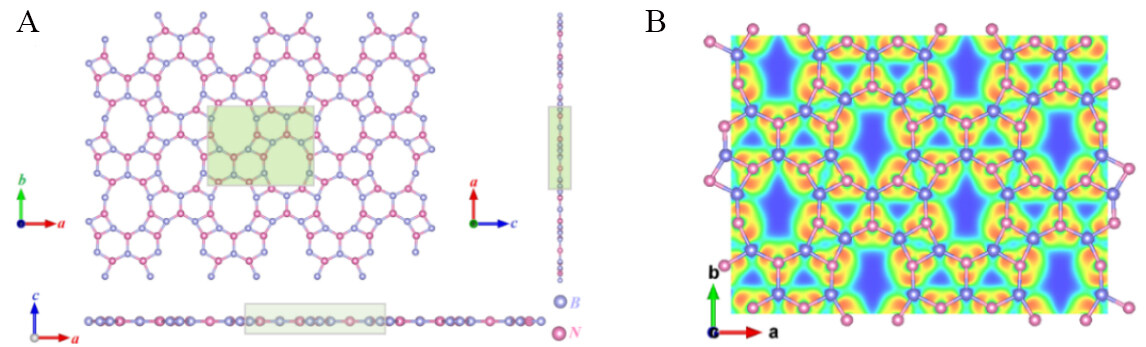
Figure 1. (A) Top and side views of optimized Pmma BN atomic structure. (B) ELF for Pmma BN with an isosurface value of 1.
Lattice constants (Å), in-plane elastic constants (N/m), Young’s moduli (N/m) and Poisson’s ratios along the x and y directions for Pmma BN under uniaxial strain
| Uniaxial strain | a | b | C11 | C22 | C12 | C44 | Ex | Ey | vx | vy | |
| Pmma BN | 0% | 9.13 | 6.77 | 195 | 256 | 58 | 34 | 182 | 239 | 0.23 | 0.29 |
| 5% (x-axis) | 9.58 | 6.77 | 183 | 231 | 42 | 67 | |||||
| 10% (x-axis) | 10.04 | 6.77 | 158 | 205 | 28 | 5 | |||||
| 15% (x-axis) | 10.50 | 6.77 | 115 | 184 | 15 | 59 | |||||
| 5% (y-axis) | 9.13 | 7.11 | 176 | 215 | 39 | 12 | |||||
| 10% (y-axis) | 9.13 | 7.45 | 154 | 159 | 23 | 20 | |||||
| 15% (y-axis) | 9.13 | 7.79 | 133 | 92 | 10 | 24 | |||||
| B4N[39] | 0% | 153 | 267 | -4.9 | 153 | 268 | -0.02 | -0.03 | |||
| h-BN[40] | 0% | 290 | 290 | 64 | 276 | 276 | 0.22 | 0.22 |
The stability of the novel 2D BN in the Pmma phase is demonstrated by phonon spectra, AIMD simulations and elastic constants. The phonon spectra of Pmma BN are shown in Figure 2A, with no imaginary frequencies exhibited, thereby proving its dynamic stability. We next investigated the thermal stability of Pmma BN and AIMD simulations were performed with a 3 × 4 × 1 supercell of Pmma BN for 4 ps at 300 and 500 K. The results are illustrated in Figure 2B and the atomic configurations at the end of the 4 ps AIMD simulations illustrated in Figure 2C demonstrate that we find no significant structural distortions at 300 and 500 K and observe no B−N bond breakage during the simulations or phase transitions. This indicates that Pmma BN is thermally stable up to at least 500 K.
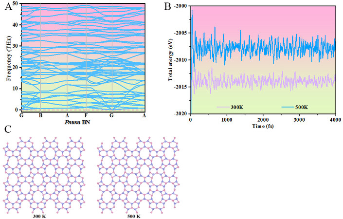
Figure 2. (A) Phonon spectra of Pmma BN. (B) Fluctuations in total energy as a function of AIMD simulations at 300 and 500 K of Pmma BN. (C) Atomic configurations at the end of the 4 ps AIMD simulations.
This work obtains the in-plane elastic constants C11, C22, C12 and C44 of 2D materials by the second partial derivative of the elastic energy in Equation (1)[43]:

The three-dimensional plot of the strain-energy surface is shown in Figure 3 and the values of the calculated in-plane elastic constants of Pmma BN are displayed in Table 1. The elastic constants of 2D crystals should satisfy Equations (2) and (3)[44]:


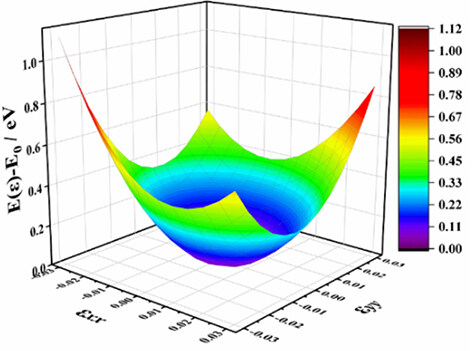
Figure 3. Three-dimensional plot of strain-energy surface.
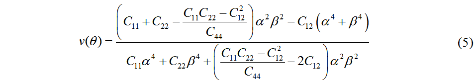
Clearly, the fact that these values satisfy the mechanical stability criteria demonstrates that Pmma BN is mechanically stable. According to the in-plane elastic constants of a 2D material, the in-plane Young’s modulus (E) and Poisson’s ratio (v) along an arbitrary direction θ (angle referring to the x direction) can be obtained by Equations (4) and (5)[43]:

where α = sin θ and β = cos θ.
The orientation dependences of the Young’s modulus and Poisson’s ratio of Pmma BN are shown in Figure 4. The shape displayed in Figure 4 deviates greatly from the circle, which implies that Pmma BN has relatively large anisotropy with regards to the Young’s modulus and Poisson’s ratio. The largest Young’s modulus appears in the y direction, while the smallest Young’s modulus appears in the x + y direction. This indicates that Pmma BN deforms more easily along the x + y direction. Poisson’s ratio is 0.23 along the x direction and 0.29 in the y direction, indicating that the expansion of the latter is smaller under tensile strain. For comparison, the calculated mechanical properties of the B4N monolayer and h-BN are also shown in Table 1. The in-plane Young’s moduli along the x and y directions of the B4N monolayer are 153 and 268 N/m, respectively, exposing a stronger anisotropy than Pmma BN. However, the Young’s modulus and Poisson’s ratio along the x and y directions of h-BN are equal, indicating that it is isotropic.
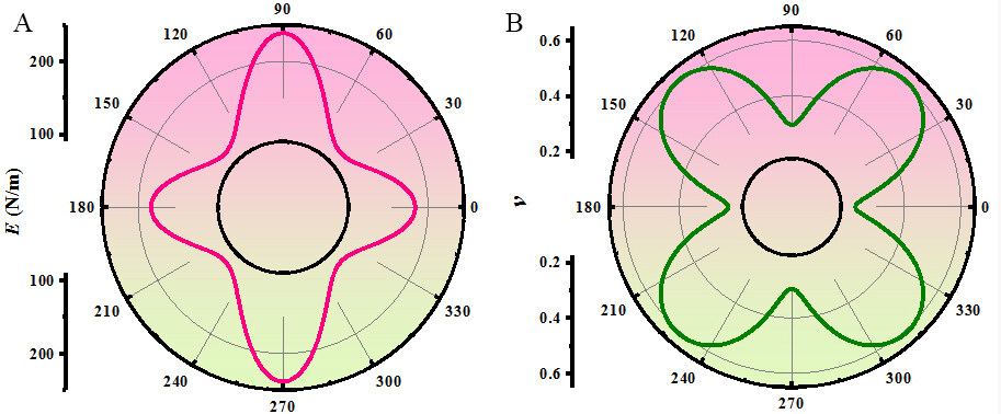
Figure 4. Orientation dependences of (A) Young’s modulus and (B) Poisson’s ratio for Pmma BN.
We next analyze the electronic properties of Pmma BN through the band structure, band decomposed charge densities at the conduction band minimum (CBM) and valence band maximum (VBM) and the effective mass anisotropy of holes and electrons. Figure 5A exhibits the electric band structure and partial density of states (PDOS) of Pmma BN. The CBM is located between the G point (0, 0, 0) and the B point (0.5, 0, 0), while the VBM is located between the F point (0, 0.5, 0) and the G point. The results show that Pmma BN is an indirect band gap semiconductor material with a band gap of 5.15 eV. Although the G point may also appear to be the VBM, it is actually 0.015 eV lower in energy than the VBM between the F and G points. As shown in the PDOS, the CBM of Pmma BN mainly consists of B-pz orbitals, while the VBM mainly consists of N-pz orbitals.
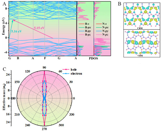
Figure 5. (A) Electronic band structure and PDOS of Pmma BN. (B) Band-decomposed charge densities at the VBM and CBM. The isosurface value is 0.025 eV/Å3. (C) Orientation-dependent carrier effective mass. The angle refers to the x direction.
The decomposed charge density at the CBM and VBM is shown in Figure 5B. The charge density is located around the B and N atoms at the CBM and around the N atoms at the VBM. This suggests that the VBM is entirely dominated by the N atoms, while the CBM is mainly dominated by the N atoms. The effective mass and mobility of carriers are important parameters for characterizing the carrier transport properties of semiconductor materials. Based on the effective mass approximation and the electroacoustic phonon scattering mechanism, the carrier mobility of 2D materials can be obtained by Equation (6)[45,46]:

where C2D is the in-plane elastic constant. The effective masses m* of electrons and holes are obtained by Equation (7), which fits the band edge dispersions at the CBM and VBM, respectively[47]:

where me* = (mx* my*)1/2 is the average effective mass and mx* and my* are the effective masses in the x and y directions, respectively.
The effective mass anisotropy of holes and electrons is displayed in Figure 5C. The angle refers to the x direction and the variation factor of the hole and electron effective masses is 5. The hole and electron effective masses show high anisotropy, with a minimum in the x direction (0.61/0.39 m0) and a maximum in the y direction (26.63/17.46 m0). The hole effective mass is greater than the electron effective mass in both the x and y directions. The obtained results of C2D, md*, E1, and μd for electrons and holes along the x and y directions are shown in Table 2. E1 is the deformation potential constant, which is obtained by the linear fits to the band-edge positions ECBM and EVBM are with respect to the vacuum energy Evacuum as a function of lattice compression or dilatation. E1x and E1y represent the deformation potential constants along the x and y directions, respectively. The energy variations of the CBM and VBM with uniaxial strain using a step of 0.5% are presented in Figure 6. From Table 2, the carrier mobilities for electrons in Pmma BN are almost the same along the x and y directions, while the value for holes along the y direction is more than double the value along the x direction.
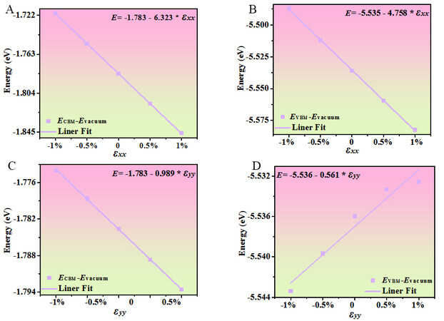
Figure 6. (A) ECBM and (B) EVBM of Pmma BN relative to the vacuum energy Evacuum as a function of small uniaxial strain along the x direction. (C) ECBM and (D) EVBM of Pmma BN relative to the vacuum energy Evacuum as a function of small uniaxial strain along the y direction.
In-plane elastic constants C2D (N/m), effective mass md* (in me), deformation potential E1 (eV) and carrier mobility μd(cm2 V-1 s-1) of holes and electrons in Pmma BN
| Carrier types | Cx | Cy | mx*/m0 | my*/m0 | E1x | E1y | μx | μy |
| Electrons | 195 | 256 | 0.39 | 17.46 | 6.32 | 0.98 | 143 | 172 |
| Holes | 195 | 256 | 0.61 | 26.63 | 4.76 | 0.56 | 106 | 228 |
In addition, we investigate the effect of uniaxial tensile strain on Pmma BN. Table 1 lists the in-plane elastic constants for Pmma BN under uniaxial strain. For C11, C22, and C12, the values gradually decrease as the uniaxial strain increases. In addition, the change in the elastic constant is more pronounced with increasing uniaxial strain along the y-axis relative to applying uniaxial strain along the x-axis. Applying uniaxial strain along the y-axis increases the value of C44, whereas increasing the uniaxial strain along the x-axis irregularly changes the value of C44 and when 10% uniaxial strain is applied along the x-axis, the value of C44 becomes small with a value of only 5. Fortunately, the in-plane elastic constants of Pmma BN under uniaxial strain are consistent with the mechanical stability criterion of 2D materials and are all mechanically stable.
The fracture strength of Pmma BN is studied by calculating the variation in stress with uniaxial tensile strain. As seen from the strain-stress curves in Figure 7A, the maximum stresses are 24.02 N/m at 17.5% uniaxial strain along the y direction and 23.74 N/m at 22% uniaxial strain along the x direction. A fracture occurs when the uniaxial strain reaches 18.5% along the y direction. After that, the effect of uniaxial tensile strain on lattice stability is further studied by calculating the phonon spectra with increasing uniaxial strain increases. As shown in Figure 7B, there are no imaginary phonon modes of the phonon spectra at 19% uniaxial strain along the x direction, while it appears in the figure when the uniaxial strain along the x direction increases to 20%. Figure 7C shows that the phonon spectra have no imaginary phonon modes at 18% uniaxial strain along the y direction but have imaginary phonon modes when the uniaxial strain along the y direction is 19%. This indicates that the lattice of Pmma BN becomes unstable when the uniaxial strain along the x and y directions is 20% and 19%, respectively, while the higher fracture strain is beneficial to the future application of this material in strain engineering.
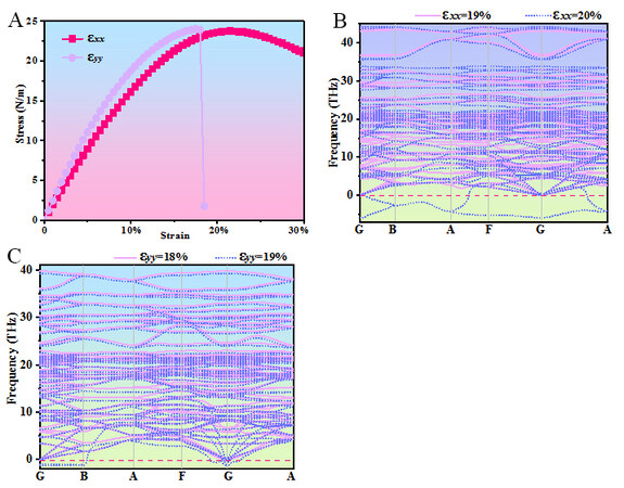
Figure 7. (A) Strain-stress curves for uniaxial tensile strain in Pmma BN. (B) Phonon spectra at 19% and 20% uniaxial strains along the x direction. (C) Phonon spectra at 18% and 19% uniaxial strains along the y direction.
Using the HSE06 functional, we calculate the band structure of Pmma BN and study the effect of uniaxial strain on its electronic properties. The uniaxial strain along the x direction of the band structure is up to 19%, while the uniaxial strain along the y direction is up to 18% and the step length is 1%. The band structures with uniaxial strains of 0%, 5%, 10%, 15%, and 19% along the x direction are shown in Figure 8A. The band gap under uniaxial strain along the x direction is shown in Figure 8B. The band gaps of Pmma BN remain indirect under uniaxial strain and the uniaxial strain applied along the x direction makes the band gap gradually smaller. When the uniaxial strain along the x direction reaches 19%, the band gap is the smallest at 4.51 eV. The band gap adjustable range of Pmma BN at the uniaxial strain along the x direction reaches 0.64 eV. Figure 8C exhibits the band structures with uniaxial strains of 0%, 1%, 2%, 10% and 18% along the y direction. When 1% uniaxial strain is applied along the y direction, the CBM is transferred from the G and B points to the G and A points (0.5, 0.5, 0) and the band gap decreases by 0.02 eV. When the uniaxial strain is applied to 2% along the y direction, the CBM occurs between the A and F points, while the VBM is transferred from the F and G points to the G point and the band gap decreases to 5.08 eV. The band gap under uniaxial strain along the y direction is shown in Figure 8D. The band gap decreases to 4.58 eV (18%) as the uniaxial strain increases along the y direction.
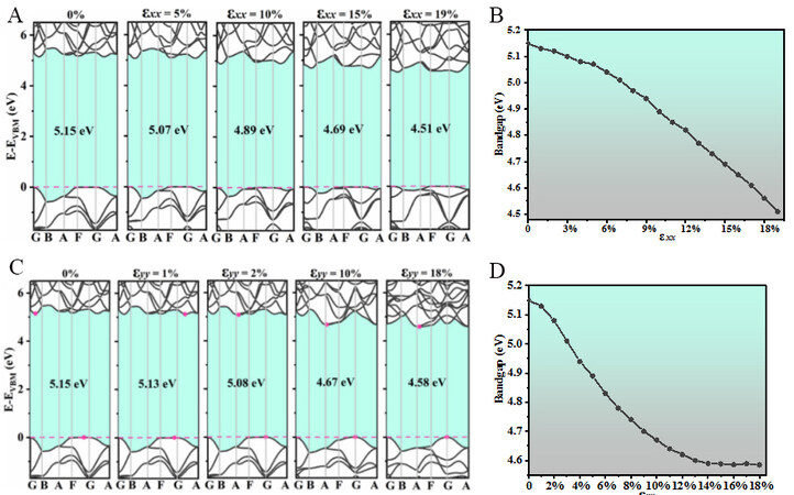
Figure 8. (A) Electronic band structures of Pmma BN under 0%, 5%, 10%, 15% and 19% uniaxial strain along the x direction. (B) Band gap under uniaxial strain along the x direction. (C) Electronic band structures under 0%, 1%, 2%, 10% and 18% uniaxial strain along the y direction. (D) Band gap under uniaxial strain along the y direction.
To explore its possible application fields, the optical absorption spectra of Pmma BN under uniaxial strain with a step size of 2% are studied by Cambridge Serial Total Energy Package (CASTEP)[48] and PBE[33] functional. Since the spectral lines do not change significantly with a step size of 2%, in order to make the optical absorption spectra look clearer, we plotted Figure 9 with a step size of 4%. Obviously, Pmma BN and its structures under uniaxial strain have a strong optical absorption capacity in the ultraviolet region. Figure 9A and B show the optical absorption spectra of Pmma BN under uniaxial strain along the x and y direction, respectively. For the x direction, the optical absorption spectra exhibit a slight red shift and a promising increase in absorption in the visible region, which is mainly caused by the contraction of the band gap under uniaxial strain. For the y direction, the increase in uniaxial strain significantly improves the optical absorption capacity of Pmma BN after 100 nm in the optical absorption spectra. The optical absorption spectra indicate that applying uniaxial strain along the y direction has a greater effect on the optical absorption capacity of Pmma BN in the ultraviolet region. The adjustable wide band gap and strong optical absorption in the ultraviolet region may allow Pmma BN to meet the needs of photodetectors.
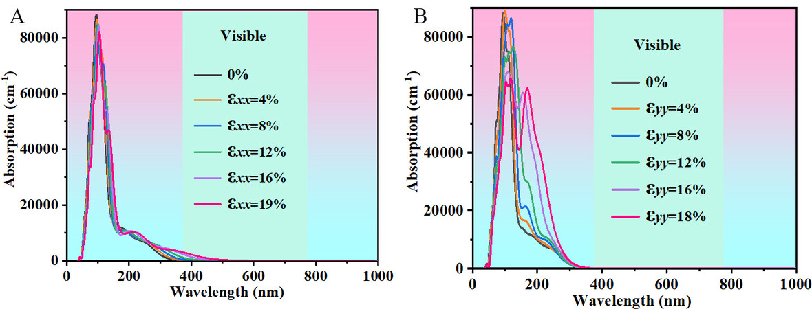
Figure 9. Absorption spectra of Pmma BN under uniaxial strain along the (A) x direction and the (B) y direction.
Finally, considering the increasing importance of green energy production, the thermoelectric properties, such as the electrical conductivity, Seebeck coefficient, phononic thermal conductivity, and thermoelectric figure of merit (ZT), of Pmma BN under uniaxial strain in the temperature range of 50–1950 K are studied. The results as a function of temperature are displayed in Figure 10. A large Seebeck coefficient and electrical conductivity and a small thermal conductivity favor high-performance thermoelectric materials. As seen from Figure 10A, Pmma BN has the largest electrical conductivity at 18% uniaxial strain along the y direction and the smallest electrical conductivity at 19% uniaxial strain along the x direction. From Figure 10B, the Seebeck coefficients of Pmma BN under uniaxial strain are similar at 50–250 K and Pmma BN without uniaxial strain has the largest Seebeck coefficient after 250 K. In Figure 10C and D, the phononic thermal conductivity and ZT show a monotonic increase with temperature for Pmma BN under uniaxial strain. Additionally, the ZT of Pmma BN without uniaxial strain after 250 K increases more rapidly than others and reaches 0.54 at 1950 K. The results demonstrate that the application of uniaxial strain reduces the thermoelectric figure of merit of Pmma BN and affects the thermoelectric properties. Therefore, when making a heterojunction, the lattice match should be as small as possible.
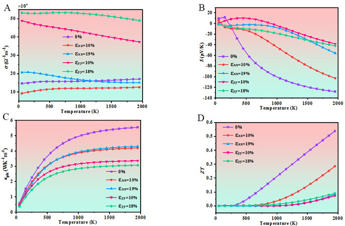
Figure 10. Pmma BN under uniaxial strain: (A) electrical conductivity; (B) Seebeck coefficient; (C) phononic thermal conductivity; (D) thermoelectric figure of merit.
CONCLUSIONS
In this study, a new type of 2D boron nitride named Pmma BN is proposed and studied using first-principles calculations. First, the dynamic, thermal, and mechanical stability of the novel 2D BN in the Pmma phase are demonstrated by phonon spectra, AIMD simulations, and elastic constants. Second, the orientation dependences of the Young’s modulus and Poisson’s ratio of Pmma BN show that it has mechanical anisotropy. Additionally, Pmma BN is an indirect band gap semiconductor material with a band gap of 5.15 eV and the hole and electron effective masses show high anisotropy. The electron carrier mobility of Pmma BN along the x and y directions is basically the same, while the hole carrier mobility along the y direction is more than double that along the x direction. The influence of uniaxial strain on the physical properties of BN is then studied. The band gaps of Pmma BN remain indirect under uniaxial strain and its adjustable range at the uniaxial strain along the x direction reaches 0.64 eV. When 2% uniaxial strain is applied along the y direction, the CBM is between A and F points, the VBM is transferred from the F and G points to the G point and the band gap is reduced to 5.08 eV. Pmma BN under uniaxial strain shows strong optical absorption capacity in the ultraviolet region. Finally, considering the increasing importance of green energy production, the thermoelectric properties of Pmma BN show that the application of uniaxial strain reduces its ZT and affects its thermoelectric properties. Therefore, these results provide a new 2D boron nitride material with excellent material properties for possible applications.
DECLARATIONS
AcknowledgementsSong Y (School of Microelectronics, Xidian University) is thanked for allowing use of the CASTEP code in Materials Studio. We gratefully acknowledge HZWTECH for providing computation facilities.
Authors’ contributionsFunding acquisition: Fan Q, Yun S
Investigation: Fan Q, Zhou H, Zhao Y, Yun S
Writing – original draft: Fan Q, Zhou H
Project administration: Fan Q
Availability of data and materialsThe data that support the findings of this study are available from the corresponding author upon reasonable request.
Financial support and sponsorshipThis work was supported by the National Natural Science Foundation of China (No. 61804120); China Postdoctoral Science Foundation (No. 2019TQ0243, No. 2019M663646); Natural Science Basic Research Program of Shaanxi (Program No. 2021JQ-515), Key Science and Technology Innovation Team of Shaanxi Province (2022TD-34), Key Scientific Research Plan of Education Department of Shaanxi Provincial Government (Key Laboratory Project) (No. 20JS066), Scientific Research Program of Shaanxi Provincial Education Department (No. 19JK0471); Young Talent Fund of University Association for Science and Technology in Shaanxi, China (No. 20190110); National Key R&D Program of China (No. 2018YFB1502902); and Key Program for International S&T Cooperation Projects of Shaanxi Province (No. 2019KWZ-03).
Conflicts of interestAll authors declared that there are no conflicts of interest.
Ethical approval and consent to participateNot applicable.
Consent for publicationNot applicable.
Copyright© The Author(s) 2022.
REFERENCES
1. Novoselov KS, Morozov SV, Jiang D. Electric field effect in atomically thin carbon films. Science 2004;306:666.
2. Novoselov KS, Geim AK, Morozov SV, et al. Two-dimensional gas of massless Dirac fermions in graphene. Nature 2005;438:197-200.
3. Mounet N, Gibertini M, Schwaller P, et al. Two-dimensional materials from high-throughput computational exfoliation of experimentally known compounds. Nat Nanotechnol 2018;13:246-52.
4. Xu R, Zou X, Liu B, Cheng H. Computational design and property predictions for two-dimensional nanostructures. Mater Today 2018;21:391-418.
5. Ma Y, Li B, Yang S. Ultrathin two-dimensional metallic nanomaterials. Mater Chem Front 2018;2:456-67.
6. Choi W, Choudhary N, Han GH, Park J, Akinwande D, Lee YH. Recent development of two-dimensional transition metal dichalcogenides and their applications. Mater Today 2017;20:116-30.
7. Dong R, Kuljanishvili I. Review Article: progress in fabrication of transition metal dichalcogenides heterostructure systems. J Vac Sci Technol B Nanotechnol Microelectron 2017;35:030803.
8. Manzeli S, Ovchinnikov D, Pasquier D, Yazyev OV, Kis A. 2D transition metal dichalcogenides. Nat Rev Mater 2017:2.
9. Kolobov AV, Tominaga J. Two-dimensional transitionmetal dichalcogenides. SPRINGER 2018; doi: 10.1007/978-3-319-31450-1.
10. Illarionov YY, Knobloch T, Jech M, et al. Insulators for 2D nanoelectronics: the gap to bridge. Nat Commun 2020;11:3385.
11. Neto AH, Guinea F, Peres NMR, Novoselov KS, Geim AK. The electronic properties of graphene. Rev Mod Phys 2009;81:109-62.
12. Liu J, Liu Z, Song T, Cui X. Computational search for two-dimensional intrinsic half-metals in transition-metal dinitrides. J Mater Chem C 2017;5:727-32.
13. Ashton M, Gluhovic D, Sinnott SB, Guo J, Stewart DA, Hennig RG. Two-dimensional intrinsic half-metals with large spin gaps. Nano Letters 2017;17:5251.
14. Wang S, Yu Z, Liu Y, et al. Two-dimensional nodal-loop half-metal in monolayer MnN. Phys Rev Materials 2019:3.
15. Saito Y, Nojima T, Iwasa Y. Highly crystalline 2d superconductors. Nat Rev Mater 2016;2(1):16094.
16. Fan Q, Yan L, Tripp MW, et al. Biphenylene network: a nonbenzenoid carbon allotrope. Science 2021;372:852-6.
17. Li G, Li Y, Liu H, Guo Y, Li Y, Zhu D. Architecture of graphdiyne nanoscale films. Chem Commun (Camb) 2010;46:3256-8.
18. Jia Z, Zuo Z, Yi Y, et al. Low temperature, atmospheric pressure for synthesis of a new carbon Ene-yne and application in Li storage. Nano Energy 2017;33:343-9.
19. Li X, Zhang H, Chi L. On-surface synthesis of graphyne-based nanostructures. Adv Mater 2019;31:e1804087.
20. Zheng C, Zhu J, Yang C, Lu C, Chen Z, Zhuang X. The art of two-dimensional soft nanomaterials. Sci China Chem 2019;62:1145-93.
21. Miao L, Jia R, Wang Y, et al. Certain doping concentrations caused half-metallic graphene. J Saudi Chem Soc 2017;21:111-7.
22. Yang D, Tian Z, Chen Y, Eglitis RI, Zhang H, Jia R. Giant piezoelectricity in B/N doped 4,12,2-graphyne. Appl Surf Sci 2020;499:143800.
23. Ong WJ, Tan LL, Ng YH, Yong ST, Chai SP. Graphitic Carbon Nitride (g-C3N4)-based photocatalysts for artificial photosynthesis and environmental remediation: are we a step closer to achieving sustainability? Chem Rev 2016;116:7159-329.
25. Chen X, Zhao J, Li G, Zhang D, Li H. Recent advances in photocatalytic renewable energy production. Energy Mater 2022; doi: 10.20517/energymater.2021.24.
26. Novoselov KS, Jiang D, Schedin F, et al. Two-dimensional atomic crystals. Proc Natl Acad Sci USA 2005;102:10451-3.
28. Lee KH, Shin HJ, Lee J, et al. Large-scale synthesis of high-quality hexagonal boron nitride nanosheets for large-area graphene electronics. Nano Lett 2012;12:714-8.
29. Pontes J, Frazão N, Azevedo DL, Lima JR. Electronic, optical, vibrational and thermodynamic properties of phaBN structure: a first principles study. Comput Mater Sci 2021;188:110210.
30. Li F, Yang D, Qiao L, et al. Novel 2D boron nitride with optimal direct band gap: a theoretical prediction. Appl Surf Sci 2022;578:151929.
31. Kresse G, Furthmüller J. Efficiency of ab-initio total energy calculations for metals and semiconductors using a plane-wave basis set. Comput Mater Sci 1996;6:15-50.
32. Kresse G, Furthmüller J. Efficient iterative schemes for ab initio total-energy calculations using a plane-wave basis set. Phys Rev B Condens Matter 1996;54:11169-86.
33. Perdew JP, Burke K, Ernzerhof M. Generalized gradient approximation made simple. Phys Rev Lett 1996;77:3865-8.
34. Pfrommer BG, Côté M, Louie SG, Cohen ML. Relaxation of crystals with the quasi-newton method. J Comput Phys 1997;131:233-40.
35. Heyd J, Scuseria GE, Ernzerhof M. Hybrid functionals based on a screened Coulomb potential. J Chem Phys 2003;118:8207-15.
36. Gonze X, Vigneron J. Density-functional approach to nonlinear-response coefficients of solids. Phys Rev B Condens Matter 1989;39:13120-8.
37. Nosé S. A unified formulation of the constant temperature molecular dynamics methods. J Chem Phys 1984;81:511-9.
38. Taylor J, Guo H, Wang J. Ab initio modeling of quantum transport properties of molecular electronic devices. Phys Rev B 2001;63.
39. Wang B, Wu Q, Zhang Y, Ma L, Wang J. Auxetic B4N Monolayer: a Promising 2D material with in-plane negative poisson’s ratio and large anisotropic mechanics. ACS Appl Mater Interfaces 2019;11:33231-7.
40. Andrew RC, Mapasha RE, Ukpong AM, Chetty N. Mechanical properties of graphene and boronitrene. Phys Rev B 2012:85.
41. Silvi B, Savin A. Classification of chemical bonds based on topological analysis of electron localization functions. Nature 1994;371:683-6.
42. Becke AD, Edgecombe KE. A simple measure of electron localization in atomic and molecular systems. J Chem Phys 1990;92:5397-403.
43. Cadelano E, Palla PL, Giordano S, Colombo L. Elastic properties of hydrogenated graphene. Phys Rev B 2010:82.
44. Ding Y, Wang Y. Density functional theory study of the silicene-like SiX and XSi3 (X = B, C, N, Al, P) honeycomb lattices: the various buckled structures and versatile electronic properties. J Phys Chem C 2013;117:18266-78.
45. Price P. Two-dimensional electron transport in semiconductor layers. I. Phonon scattering. Annals of Physics 1981;133:217-39.
46. Qiao J, Kong X, Hu ZX, Yang F, Ji W. High-mobility transport anisotropy and linear dichroism in few-layer black phosphorus. Nat Commun 2014;5:4475.
47. Wang S, Li J, Zhu X, Wang M. A new two-dimensional semiconducting carbon allotrope: a first-principles study. Carbon 2019;143:517-22.
Cite This Article
Export citation file: BibTeX | RIS
OAE Style
Fan Q, Zhou H, Zhao Y, Yun S. Predicting a novel two-dimensional BN material with a wide band gap. Energy Mater 2022;2:200022. http://dx.doi.org/10.20517/energymater.2022.21
AMA Style
Fan Q, Zhou H, Zhao Y, Yun S. Predicting a novel two-dimensional BN material with a wide band gap. Energy Materials. 2022; 2(3): 200022. http://dx.doi.org/10.20517/energymater.2022.21
Chicago/Turabian Style
Fan, Qingyang, Hang Zhou, Yingbo Zhao, Sining Yun. 2022. "Predicting a novel two-dimensional BN material with a wide band gap" Energy Materials. 2, no.3: 200022. http://dx.doi.org/10.20517/energymater.2022.21
ACS Style
Fan, Q.; Zhou H.; Zhao Y.; Yun S. Predicting a novel two-dimensional BN material with a wide band gap. Energy Mater. 2022, 2, 200022. http://dx.doi.org/10.20517/energymater.2022.21
About This Article
Copyright

Data & Comments
Data


 Cite This Article 11 clicks

 Like This Article 36
likes
Like This Article 36
likes


Comments
Comments must be written in English. Spam, offensive content, impersonation, and private information will not be permitted. If any comment is reported and identified as inappropriate content by OAE staff, the comment will be removed without notice. If you have any queries or need any help, please contact us at support@oaepublish.com.