
Homojunction perovskite solar cells: opportunities and challenges


Abstract
Organometallic halide perovskites have rapidly become promising materials as a result of their outstanding properties in high-efficiency and low-cost next-generation solar cells. Perovskite materials can be adjusted to be p- or n-type by defect engineering through, for example, the self-doping method by controlling the precursor compositions and process conditions. Recently, a p-type perovskite/n-type perovskite homojunction has been proposed and constructed, which provides a possibility for the design of a novel type of perovskite solar cell (PSC). Following a brief overview of the physical fundamentals of perovskite homojunctions, a detailed discussion of the promising progress of recently reported homojunction PSCs is presented here, including theoretical simulations, extrinsic and interfacial doping and graded structures. Furthermore, the opportunities regarding higher doping concentrations, simpler device architectures, ion migration inhibition and device stability are discussed. Finally, an outlook that offers insights into the future development of highly efficient and stable homojunction PSCs is provided.
Keywords
INTRODUCTION
Organometallic halide perovskites have become prominent semiconductor materials in recent years due to their excellent optical and electrical characteristics. So far, perovskite materials have been utilized to realize high-performance solar cells[1,2], light-emitting diodes[3,4], photoelectric sensors[5,6] and other devices[7-10], most of which are based on heterojunction structures. Perovskite materials also benefit from their unprecedented ability to regulate their physical properties, including dimensions[11], direct bandgap[12] and electronically benign defects[13,14]. In particular, p- or n-type perovskite films can be fabricated by defect engineering through, for example, self-doping by controlling the precursor compositions and process conditions. Furthermore, the perovskite p-n homojunction structure[15] was proposed and demonstrated by precise regulation of the precursor stoichiometry. This homojunction was further integrated into planar perovskite solar cells (PSCs) to obtain excellent performance by introducing internal electric fields within the perovskite absorber layer[15]. Since then, researchers have dedicated significant attention to the perovskite homojunction architecture and investigated the electrical doping of perovskite materials[16], such as the conductivity type (p or n) and density of carriers.
The p-n junction is the basis of the semiconductor industry. The p-n homojunction is a junction between layers of similar materials with different doping types. The most common semiconductor materials, such as Si, Ge and GaAs, have excellent ambipolar doping characteristics, so they can form homojunction devices with outstanding performance. Similarly, the electrical doping of perovskite materials provides the possibility of perovskite homojunctions. Park et al.[17] reported the fabrication of homojunction PSCs with defect management by Cui et al.[15], thereby opening a new avenue for metal halide perovskite devices. Beyond existing planar heterojunction PSCs, the advent of perovskite homojunctions has brought an effective fresh route to achieve high power conversion efficiencies (PCEs) for PSCs. Moreover, perovskite homojunctions can draw on the mature experience and technologies established for classical inorganic solar cells, like silicon[18], which rely on homojunctions. Hence, homojunction PSCs have significant development prospects.
Although research into perovskite homojunction devices is still in its infancy, numerous high-quality studies continue to advance this field, as discussed in the following sections. Through simulation analysis, studies on performance optimization, structure design and defect management of homojunction PSCs provide theoretical guidance for this field. Moreover, experimental studies on extrinsic metal ion doping technology, interfacial doping strategies and graded homojunction designs have further expanded the development of perovskite homojunctions. Here, we introduce the physical fundamentals of perovskite homojunctions, further elucidate the significant research progress made so far, discuss research hot spots and opportunities and analyze the current technical bottlenecks to provide a critical reference for the development of PSCs.
FUNDAMENTALS OF PEROVSKITE HOMOJUNCTIONS: ELECTRICAL DOPING
Electrical doping is an important feature of optoelectronic semiconductor materials. The p- or n-type conductive properties of perovskite materials can be principally changed by intrinsic defects and extrinsic doping, resulting in the generation of holes or electrons. Intrinsic defects are mainly represented by point defects in the perovskite materials [Figure 1A] and can be induced and controlled through various methods, such as the film growth conditions[20], the temperature and time of the annealing treatment[21], the irradiation intensity[22] and the proportion of precursor components[19]. For example, there are numerous possible point defects in MAPbI3 perovskite, including three vacancies (VMA, VPb and VI), three interstitials (MAi, Pbi and Ii), two cation substitutions (MAPb and PbMA) and four antisite substitutions (MAi, Pbi, IMA and IPb). It is reported that Ii, MAi, VMA, VPb, MAPb, PbMA and VI have low formation energies and can easily occur in bulk perovskite materials[23] [Figure 1B]. Among these defects, VI, MAi and MAPb can promote the transformation of perovskite films to n-type doping, while VPb and PbMA can lead to p-type doping.
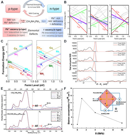
Figure 1. Characteristics of electrical doping. (A) Schematic of conductivity type conversions in perovskite films by self-doping. Reproduced from Wang et al.[19]. (B) Formation energies of intrinsic point defects in MAPbI3, where the vertical dotted lines indicate Fermi level pinning and the Fermi levels are referenced to the valence band maximum. Reproduced from Yin et al.[23]. (C) Calculated formations energies of defects formed by group IA and IB elements as a function of the Fermi level under I-rich/Pb-poor and I-poor/Pb-rich conditions. (D) Calculated total density of states (DOS) and partial DOS for OI, SI, SeI, and TeI acceptors. Reproduced from
In contrast, extrinsic doping occurs via the introduction of impurity atoms to a crystal structure. For example, MAPbI3 can be regulated by introducing elements of the first main group (IA), the first subgroup (IB) and the sixth main group (VIA)[24] [Figure 1C and D]. The introduction of Na, K, Rb, Cu and O elements (substitutionally or interstitially) can form accepter impurities under the conditions of I-rich or Pb-poor, which can cause the Fermi energy level (EF) of perovskite films to move down, i.e., p-type doping. Furthermore, n-type doping can be achieved through the partial substitution of Pb in perovskites with Sb or Sn[25], or the partial substitution of halogen group elements I in perovskite by Cl[26] [Figure 1E and F]. Hence, appropriate intrinsic and extrinsic defect strategies are key to tuning the carrier concentration and Fermi level position in perovskite materials for homojunction formation.
Aside from the conductivity type and the carrier density of the semiconductor, electrical doping can also affect the carrier mobility and recombination lifetime, extraction and injection of charge and further the photoelectric performance of devices. Therefore, doping methods play a key role in optimizing perovskite materials and improving the performance of PSCs. For example, Han et al.[28] introduced CaCl2 into
RECENT ADVANCES IN HOMOJUNCTION PSCs
Characterization method
Doping characterization
The electrical doping of perovskite materials can be realized by self-doping or the introduction of external ions or molecules. Firstly, doping changes the electrical conductivity and the carrier density of perovskite materials. The four-probe method to measure the electrical conductivity of the perovskite film is a simple characterization of the doping level but it cannot distinguish the conductivity type. Mott-Schottky analysis can obtain information, such as conductivity type, flat band potential and donor or acceptor density through the measurement of capacitance-voltage, which has been widely used to measure the doping characteristics of perovskite materials[29,30]. It should be noted that the appropriate device structure and signal frequency need to be selected to avoid the influence of the parasitic capacitance from charge transport layers in a PSC. Moreover, by measuring the Hall effect of perovskite materials, the conductivity type and carrier density can be confirmed[31,32].
To obtain accurate results, the high resistance and low mobility characteristics of perovskite materials need to be considered. Thus, researchers have developed a variety of Hall effect measurement methods to reliably assess perovskite materials[33]. X-ray and ultraviolet photoelectron spectroscopy can measure the change in the Fermi level position of materials, effectively indicating the change in doping level and type of perovskite materials[34,35]. In addition, Kelvin probe force microscopy (KPFM) can measure the contact potential difference of the semiconductor surface and obtain the change in the work function[36,37]. KPFM can be sensitive to the surface condition of perovskite materials, so the error caused by surface contamination and other factors should be eliminated before taking the measurements. Indeed, current techniques and analytical methods have their limitations, which need to be considered and optimized to prevent misleading results. Due to the common sample-to-sample variability in perovskite materials, statistics, as well as mutual corroboration by multiple methods, are crucial to verify their characteristics.
Homojunction characterization
The identification of a homojunction can be achieved using techniques, such as cross-sectional KPFM, current-voltage (I-V) diode characterization, time-resolved photoluminescence (TRPL) spectroscopy and high-resolution transmission electron microscopy (HRTEM). The significant advantage of cross-sectional KPFM is the in situ characterization of the internal potential distribution of the device under operating conditions. This technique can be carried out under light or bias voltage to obtain obvious potential changes caused by the transfer and extraction of carriers at the junction. Furthermore, the p-n homojunction has unidirectional conductivity. Therefore, by measuring the forward and reverse I-V curves in dark conditions, the changes in the curves can determine whether there is a rectification characteristic. In addition, TRPL spectroscopy can measure photoelectron deactivation processes and deduce information regarding the carrier transfer inside the device to provide indirect proof of the junction. Aside from the electrical characteristics, p- and n-type perovskite films have differences in morphology. For example, the introduced dopants may form microcrystalline grains on the surface or be mixed into crystal lattices, thereby changing the perovskite crystallization, so HRTEM can visually observe the morphological characteristics of a homojunction. The electrical doping characterization technology is illustrated in Figure 2.
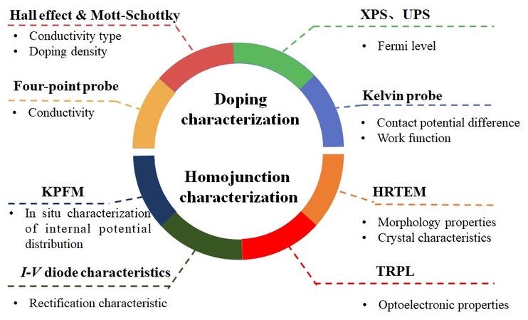
Figure 2. Current electrical doping characterization methods for perovskite thin films and homojunction structures. XSP: X-ray spectroscopy; UPS: ultraviolet photoelectron spectroscopy; KPFM: Kelvin probe force microscopy; HRTEM: high-resolution transmission electron microscopy; TRPL: time-resolved photoluminescence.
Theoretical simulation of perovskite homojunctions
Perovskite homojunctions have been constructed experimentally and show excellent application potential. Numerical simulations are fundamental in testing the feasibility and predicting the performance of a new device and can be utilized to further understand the characteristics of perovskite homojunctions. For performance optimization, Sengar et al.[38] used experimentally verified device models to study the effects of junction thickness, electric field strength and junction defect density on device performance. A stronger electric field in the homojunction can reduce the carrier recombination rate. Moreover, Li et al.[39] systematically studied the effects of different electron transport layers (ETLs) and hole transport layers (HTLs), bulk and interfacial defect densities and absorber layer thickness on the performance of perovskite homojunction devices. The performance of an optimized homojunction PSC can reach 27.10% [Figure 3A], illustrating the significant performance potential of the homojunction device. For device design,
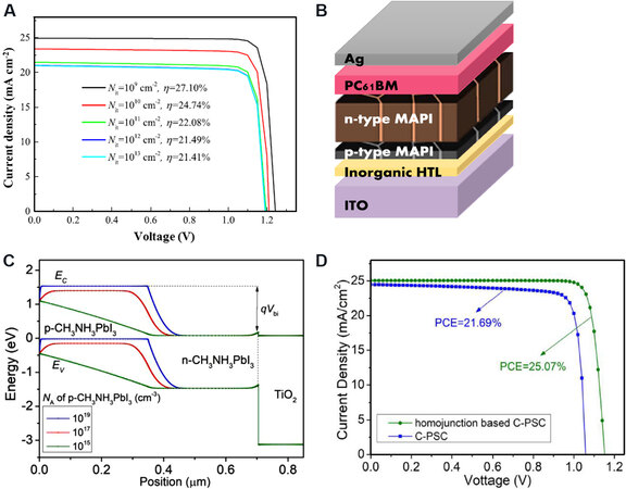
Figure 3. Simulation results of perovskite homojunction devices. (A) J-V curves with various values of NA at a p-type MAPbI3/Spiro-OMeTAD interface. Reproduced with permission from Li et al.[39]. (B) Schematic of inverted p-n homojunction PSC with ultrathin HTL. Reproduced with permission from Maram et al.[40]. (C) Energy band diagram as a function of NA in p-MAPbI3 (at fixed ND of 1017 cm-3). (D) J-V curves of optimized C-PSC and homojunction PSC. Reproduced with permission from Lin et al.[42]. PSC: Perovskite solar cell; HTL: hole transport layer.
Extrinsic doping for perovskite homojunctions
Except for the familiar self-doping strategy, extrinsic doping can also tune the carrier density and EF position in perovskite materials for the formation of perovskite homojunctions. For example, Lu et al.[43] modified the surface of a perovskite film with a trivalent metal halide salt, InBr3, converting the top surface to be more n-type. An n/n+ perovskite homojunction between the bulk [weak n-type (n) component] and the surface [stronger n-type (n+) component] was spontaneously formed [Figure 4A], with the electric field enlarged and the device performance improved [Figure 4B]. Chang et al.[44] adopted alkali metal ions (Na+, K+ and Rb+) doped in perovskite films, which changed the majority carrier type from undoped n- to p-type. The carrier density of the perovskite films was increased by at least two orders of magnitude after doping, thereby enhancing the device performance. Furthermore, Ren et al.[45] modified the surface properties of perovskite films by Ar+ bombardment [Figure 4C]. The original p-type perovskite film was transformed into n-type and a perovskite homojunction was then successfully induced in situ.
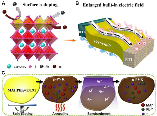
Figure 4. Extrinsic doping for perovskite homojunctions. (A, B) A simple heterovalent metal halide surface treatment strategy enables the self-assembly of an n/n+ perovskite homojunction, which synergistically enlarges the built-in electric field. Reproduced from
Interfacial doping for perovskite homojunctions
Compared with the construction of two independent high-quality perovskite films with different doping types, interfacial doping is a simpler strategy to obtain an efficient homojunction. Chen et al.[46] adopted a guanidinium bromide solution to adjust the effective doping of the surface of perovskite films. After the interfacial treatment, the junction at the perovskite/ETL interface was significantly increased [Figure 5A and B], inducing an increase in the Voc and PCE. Furthermore, Noel et al.[47] treated the perovskite film surface with a strongly oxidizing molybdenum tris(dithiolene) complex [Figure 5C], thereby shifting the work function. Xiong et al.[48] passivated the defects by using a natural additive, capsaicin, with the spontaneous formation of a perovskite p-n homojunction observed [Figure 5D-F]. The energetic transformation and defect passivation promoted charge transport at the interface, suppressed both defect-assisted recombination and interfacial carrier recombination, thereby improving the device performance.
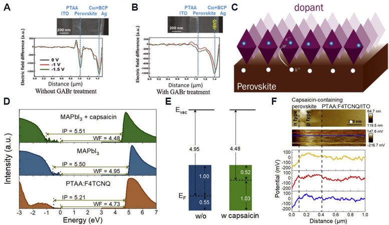
Figure 5. Interfacial doping for perovskite homojunctions. Electric field distribution as a function of depth within p-i-n PSCs (A) without and (B) with GABr treatment through cross-sectional KPFM. Reproduced from Chen et al.[46]. (C) A method for controlled p-doping of a halide perovskite surface using molecular dopants. Reproduced from Noel et al.[47]. (D, E) UPS spectra of secondary electron cutoff region and valence band region of PTAA:F4TCNQ and perovskite films with and without 0.1 wt.% capsaicin grown on PTAA:F4TCNQ. (F) Cross-sectional atomic force microscopy topographies and corresponding KPFM images and potential profiles under zero-voltage bias of perovskite/PTAA:F4TCNQ/ITO without capsaicin. Reproduced from Xiong et al.[48]. PSCs: Perovskite solar cells; KPFM: Kelvin probe force microscopy; UPS: ultraviolet photoelectron spectroscopy.
Graded structure for perovskite homojunctions
To facilitate the carrier transport in PSCs, the electric field enhancement induced by the graded junction architecture is an effective route. For both heterojunctions and homojunctions, the graded architecture with continuous band bending can construct a high-speed channel for charge transfer. For example, introducing SnI2 into perovskite films by a three-step dynamic spin coating strategy, Sun et al.[49] obtained the bandgap of the perovskite layer, which gradually decreased from 1.53 eV at the bottom to 1.27 eV at the top and the electrical doping from n- to p-type. A graded bandgap perovskite homojunction was constructed [Figure 6A], which promoted the carrier directional transport in PSCs and reduced the dependence on the ETL/HTL. Furthermore, the combination of two- (2D) and three-dimensional (3D) perovskites to prepare a graded homojunction is a method for improving the stability of PSCs. Xiang et al.[50] combined a quasi-2D PMA/Cs/FA/MA perovskite with a 3D Cs/FA/MA perovskite to construct graded perovskite homojunctions [Figure 6B and C], thereby promoting the transport and extraction of carriers and improving the PCE of the PSCs [Figure 6D]. Furthermore, Yuan et al.[51] constructed a graded perovskite quantum dot homojunction [Figure 6E] with three layers of CsPbI3, which facilitated the charge extraction and increased the carrier diffusion length due to the additional driving force of the homojunction.
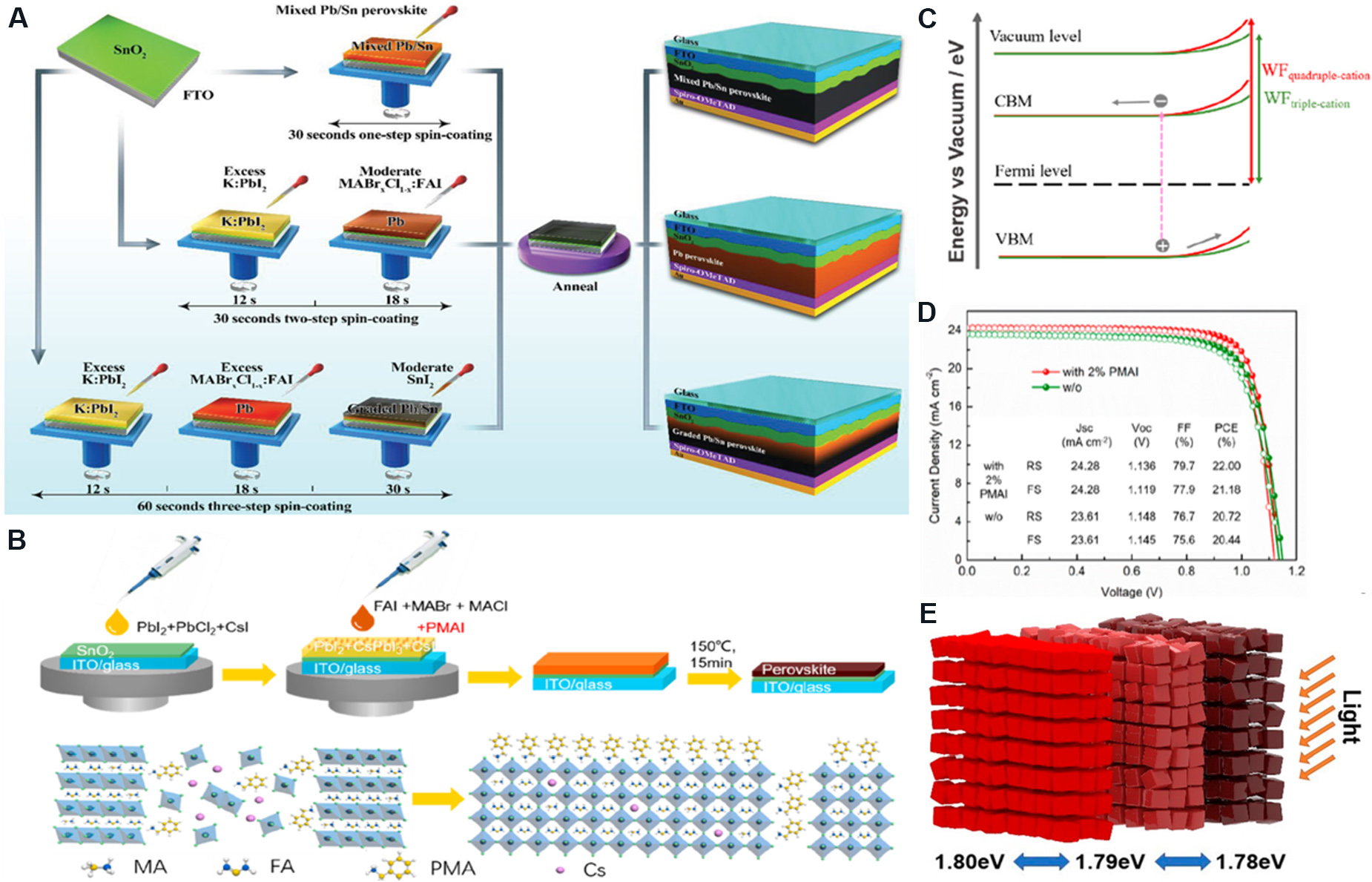
Figure 6. Preparation process, device performance and structure diagram of graded perovskite homojunction. (A) Schematic illustration of the fabrication process of mixed Pb/Sn, Pb‐based and graded Pb/Sn for graded perovskite homojunction. Reproduced with permission from Sun et al.[49]. (B) Preparation process and material structure model of perovskite. (C) Schematic band diagram of perovskite films and quadruple-cation PSCs. (D) Performance of cells with 2% PMAI and without PMAI. Reproduced with permission from Xiang et al.[50]. (E) Graded band alignment homojunction structure in solar cells. Reproduced with permission from Yuan et al.[51]. CBM: Conduction band minimum; VBM: valence band maximum.
PROMISING DIRECTIONS AND OPPORTUNITIES
Enhancing electric fields of perovskite homojunctions
The study of perovskite homojunctions is still in its infancy and requires more in-depth research to further boost device performance. Referring to the classical semiconductor theory, the carrier separation efficiency depends mainly on the built-in electric field of the junction. Theoretically, the higher doping concentration of p-/n-type perovskite layers can cause an increase in the electric field, thus enhancing the performance. Recently, Kirchartz and Cahen[52] estimated the doping densities in perovskite materials for a p-n junction and stated a minimum doping concentration of ~1016 cm-3 for a ~500 nm-thick perovskite homojunction with a built-in voltage (Vbi) of ~1 V. In fact, the traditional theory could provide a certain reference for the junction by organic-inorganic perovskite materials but the Vbi of the planar homojunction PSC reported is formed by the upper and lower charge transport layers and the perovskite homojunction together. It would be unreasonable to ignore the contribution of the ETL/HTL and only equate the homojunction with the whole device, which concluded the insufficient doping concentration of the homojunction. Certainly, further increasing the doping concentration of perovskite materials would obtain a homojunction with a stronger electric field to remove charge transport layers and obtain a pure perovskite homojunction device. In contrast, the doping concentration of MAPbI3 can reach 109-1017 cm-3 according to experimental and calculation results[25,53,54], while FASnI3[55] can reach ~1020 cm-3. Thus, perovskite materials have potential for sufficiently high doping concentrations for enhanced electric fields. However, the augment of doping concentration also leads to an increase in defect density. It is crucial to balance the relationship between high doping concentration and low defect density, which requires exploring more appropriate perovskite self-doping and extrinsic doping strategies.
Simplifying device structures
PSCs with a p-i-n structure rely on charge transport layers at both ends to selectively extract photogenerated electrons and holes. Perovskite homojunctions can achieve the selection and transport of photogenerated carriers by an built-in electric field. Therefore, the direct combination of the homojunction and electrodes can construct a very simple solar cell without the traditional ETL and HTL, thereby avoiding the expensive organic materials and complex craft process. Recently, Lin et al.[42] designed a carbon electrode perovskite homojunction solar cell without a HTL, of which the theoretical calculation results show an optimal PCE of 25%. Cui et al.[15] preliminarily tried to remove the ETL and HTL to form a simple device containing an independent homojunction with a PCE of ~8%. While simplifying the device structure, interfacial recombination becomes serious because of the direct contact between the Au electrode and perovskite film, thereby restricting the device performance. Issues, such as interfacial breakage, metal ion diffusion and carrier recombination cannot be bypassed. Therefore, it is necessary to further optimize the simple device with interfacial engineering, defect passivation, doping concentration regulation and other means for superior performance.
Challenges of ion migration
Research in the perovskite field is ever increasing, but there are still many unresolved research issues, including polarity, lattice expansion and ion migration. Current research indicates that ion migration is one of the intrinsic characteristics of organometallic halide perovskite materials. In PSCs, the numerous mobile ions in perovskite films induce phase segregation, material degradation, photocurrent hysteresis and other problems, which severely damage the carrier transfer and device stability. Thus, it is also essential to explore the ion migration influence on perovskite homojunctions for their further progress. To better understand the mobile ions in perovskite homojunctions, both theoretical and experimental advances are required to answer the following basic questions. What is the exact concentration of mobile ions in PSCs and homojunction devices? What is the precise influence of external conditions on ion migration, such as heat, light illumination, moisture and so on? What is the impact of mobile ion concentration on the performance of perovskite homojunctions?
Calado and Barnes[56] used their own software simulation to raise the question of whether a homojunction can continue operating in the presence of mobile ions. However, the extremely large ion concentration as an ideal input would result in simulation results inconsistent with the actual PSC. Homojunctions have been persistent at the common ion concentration of perovskites (e.g., less than 1017 cm-3). Moreover,
Investigating device stability
Device stability is of great importance since it is a major obstacle to the practical process of PSCs. At present, the reported homojunction PSCs demonstrate excellent operating stability. For example, Lu et al.[43] have shown a homojunction device with an enlarged built-in electric field retains more than 93% of its initial efficiency after 1000 h of maximum power point (MPP) operation, which reveals greater stability than the control device (degrading to ~80%). Sun et al.[49] evaluated the thermal stability of homojunction devices with MPP tracking under a 85 °C/85% RH environment. The devices containing the Spiro-OMeTAD break down in such a harsh environment, while the homojunction devices without HTL still work, showing a superior material stability for perovskite homojunction with graded Pb/Sn. Regarding common PSCs, numerous stability studies have focused on light, humidity, heat and oxygen factors, which are the main causes of the decomposition of perovskite crystals, resulting in a serious decrease in device performance. The common decomposition problems arising from perovskite materials may also exist in the perovskite homojunction structure. Therefore, the influencing factors (like electric field, illumination, moisture and so on) on the stability of perovskite homojunctions need to be further investigated and given special attention.
SUMMARY AND OUTLOOK
With the advantages of enhanced electric fields, effective performance improvements and simple device structures, perovskite homojunctions exhibit substantial development prospects and have therefore attracted significant interest. Here, we give a brief account of the story of perovskite homojunctions and discuss in detail the electrical doping characteristics and recent advances of perovskite homojunctions. Furthermore, the potential technical obstacles and a roadmap for perovskite homojunctions are also included and proposed.
We look forward to the extensive research on perovskite homojunctions to boost their development and practical application. Firstly, obtaining a stronger built-in electric field is critical for efficient carrier transfer in perovskite homojunctions. It is noteworthy to improve the doping concentration of perovskite materials and explore the oriented electrical doping strategy. Secondly, perovskite homojunctions provide the potential for simple devices without ETLs and HTLs. To realize more efficient PSCs, it is significant to optimize the perovskite crystalline quality and passivate the interface of the electrode and perovskite. It is then helpful to investigate the ion migration dynamics in perovskite materials and explore inhibition strategy in homojunction devices, such as low-dimensional perovskite engineering, interfacial modification, multi-defect passivation and so on. Nonetheless, it is expected that the continuing investigation of perovskite homojunctions will positively evolve and facilitate the transition of this promising technology from the laboratory to the market.
DECLARATIONS
Authors’ contributionsSupervised this research: Li M
Wrote the first manuscript: Cui P
Contributed to the discussion, review, and revision of the manuscript: Cui P, Qu S, Zhang Q, Liu B, Yan L, Du S, Wang X, Huang H, Ji J, Li M
Availability of data and materialsNot applicable.
Financial support and sponsorshipThis work is supported partially by National Natural Science Foundation of China (Grant nos. 52102245, 51772096, 51972110 and 52072121), Beijing Science and Technology Project (Z181100005118002), Par-Eu Scholars Program, Science and Technology Beijing 100 Leading Talent Training Project, Huaneng Group Headquarters Science and Technology Project, Special Project (Phase I) of Offshore Wind Power and Smart Energy System Science and Technology (HNKJ20-H88), the Fundamental Research Funds for the Central Universities (2020MS023, 2020MS028) and the NCEPU “Double First-Class” Program.
Conflicts of interestAll authors declared that there are no conflicts of interest.
Ethical approval and consent to participateNot applicable.
Consent for publicationNot applicable.
Copyright© The Author(s) 2021.
REFERENCES
1. Best Research-Cell Efficiency Chart. Available from: https://www.nrel.gov/pv/cell-efficiency.html [Last accessed on 22 Nov 2021].
2. Jeong J, Kim M, Seo J, et al. Pseudo-halide anion engineering for α-FAPbI3 perovskite solar cells. Nature 2021;592:381-5.
3. Quan LN, Rand BP, Friend RH, Mhaisalkar SG, Lee TW, Sargent EH. Perovskites for next-generation optical sources. Chem Rev 2019;119:7444-77.
4. Lu M, Zhang Y, Wang S, Guo J, Yu WW, Rogach AL. Metal halide perovskite light-emitting devices: promising technology for next-generation displays. Adv Funct Mater 2019;29:1902008.
5. Wangyang P, Gong C, Rao G, et al. Recent advances in halide perovskite photodetectors based on different dimensional materials. Advanced Optical Materials 2018;6:1701302.
6. Xie C, Liu C, Loi H, Yan F. Perovskite-based phototransistors and hybrid photodetectors. Adv Funct Mater 2020;30:1903907.
7. Yang T, Wu Q, Dai F, et al. Understanding, optimizing, and utilizing nonideal transistors based on organic or organic hybrid semiconductors. Adv Funct Mater 2020;30:1903889.
8. Liu X, Yu D, Song X, Zeng H. Metal halide perovskites: synthesis, ion migration, and application in field-effect transistors. Small 2018;14:e1801460.
9. Stylianakis MM, Maksudov T, Panagiotopoulos A, Kakavelakis G, Petridis K. Inorganic and hybrid perovskite based laser devices: a review. Materials (Basel) 2019;12:859.
10. Haque MA, Kee S, Villalva DR, Ong WL, Baran D. Halide perovskites: thermal transport and prospects for thermoelectricity. Adv Sci (Weinh) 2020;7:1903389.
11. Gao P, Bin Mohd Yusoff AR, Nazeeruddin MK. Dimensionality engineering of hybrid halide perovskite light absorbers. Nat Commun 2018;9:5028.
12. Gharibzadeh S, Abdollahi Nejand B, Jakoby M, et al. Record open-circuit voltage wide-bandgap perovskite solar cells utilizing 2D/3D perovskite heterostructure. Adv Energy Mater 2019;9:1803699.
13. Kim J, Lee SH, Lee JH, Hong KH. The role of intrinsic defects in methylammonium lead iodide perovskite. J Phys Chem Lett 2014;5:1312-7.
14. Chen Z, Dong Q, Liu Y, et al. Thin single crystal perovskite solar cells to harvest below-bandgap light absorption. Nat Commun 2017;8:1890.
15. Cui P, Wei D, Ji J, et al. Planar p-n homojunction perovskite solar cells with efficiency exceeding 21.3%. Nat Energy 2019;4:150-9.
16. Euvrard J, Yan Y, Mitzi DB. Electrical doping in halide perovskites. Nat Rev Mater 2021;6:531-49.
18. Battaglia C, Cuevas A, De Wolf S. High-efficiency crystalline silicon solar cells: status and perspectives. Energy Environ Sci 2016;9:1552-76.
19. Wang Q, Shao Y, Xie H, et al. Qualifying composition dependent p and n self-doping in CH3NH3PbI3. Appl Phys Lett 2014;105:163508.
20. Cui P, Wei D, Ji J, et al. Highly efficient electron-Selective layer free perovskite solar cells by constructing effective p-n heterojunction. Sol RRL 2017;1:1600027.
21. Ralaiarisoa M, Busby Y, Frisch J, Salzmann I, Pireaux JJ, Koch N. Correlation of annealing time with crystal structure, composition, and electronic properties of CH3NH3PbI3-xClx mixed-halide perovskite films. Phys Chem Chem Phys 2016;19:828-36.
22. Frolova LA, Dremova NN, Troshin PA. The chemical origin of the p-type and n-type doping effects in the hybrid methylammonium-lead iodide (MAPbI3) perovskite solar cells. Chem Commun (Camb) 2015;51:14917-20.
23. Yin W, Shi T, Yan Y. Unusual defect physics in CH3NH3PbI3 perovskite solar cell absorber. Appl Phys Lett 2014;104:063903.
24. Shi T, Yin W, Yan Y. Predictions for p-type CH3NH3PbI3 perovskites. J Phys Chem C 2014;118:25350-4.
25. Stoumpos CC, Malliakas CD, Kanatzidis MG. Semiconducting tin and lead iodide perovskites with organic cations: phase transitions, high mobilities, and near-infrared photoluminescent properties. Inorg Chem 2013;52:9019-38.
26. Liu Q, Hsiao Y, Ahmadi M, et al. N and p-type properties in organo-metal halide perovskites studied by Seebeck effects. Organic Electronics 2016;35:216-20.
27. Zhang J, Shang M, Wang P, et al. n-type doping and energy states tuning in CH3NH3Pb1-xSb2x/3I3 perovskite solar cells. ACS Energy Lett 2016;1:535-41.
28. Han Y, Zhao H, Duan C, et al. Controlled n-doping in air-stable CsPbI2 Br perovskite solar cells with a record efficiency of 16.79%. Adv Funct Mater 2020;30:1909972.
29. Almora O, Aranda C, Mas-marzá E, Garcia-belmonte G. On Mott-Schottky analysis interpretation of capacitance measurements in organometal perovskite solar cells. Appl Phys Lett 2016;109:173903.
30. Guerrero A, Juarez-perez EJ, Bisquert J, Mora-sero I, Garcia-belmonte G. Electrical field profile and doping in planar lead halide perovskite solar cells. Appl Phys Lett 2014;105:133902.
31. Chen Y, Yi HT, Wu X, et al. Extended carrier lifetimes and diffusion in hybrid perovskites revealed by Hall effect and photoconductivity measurements. Nat Commun 2016;7:12253.
32. Kimura T, Matsumori K, Oto K, Kanemitsu Y, Yamada Y. Observation of high carrier mobility in CH3NH3PbBr3 single crystals by AC photo-Hall measurements. Appl Phys Express 2021;14:041009.
34. Wang C, Liu X, Wang C, et al. Surface analytical investigation on organometal triiodide perovskite. Journal of Vacuum Science & Technology B 2015;33:032401.
35. Mirzehmet A, Ohtsuka T, Abd Rahman SA, Yuyama T, Krüger P, Yoshida H. Surface termination of solution-processed CH3NH3PbI3 perovskite film examined using electron spectroscopies. Adv Mater 2021;33:2004981.
36. Zheng Y, Jiang B, Gao Z, et al. Optimization of SnO2-based electron-selective contacts for Si/PEDOT:PSS heterojunction solar cells. Solar Energy 2019;193:502-6.
37. Song D, Wei D, Cui P, et al. Dual function interfacial layer for highly efficient and stable lead halide perovskite solar cells. J Mater Chem A 2016;4:6091-7.
38. Sengar BS, Garg V, Kumar A, Dwivedi P. Numerical simulation: design of high-efficiency planar p-n homojunction perovskite solar cells. IEEE Trans Electron Devices 2021;68:2360-4.
39. Li G, Guo F, Zhou X, Xue L, Huang X, Xiao Y. Performance optimization of homojunction perovskite solar cells by numerical simulation. Superlattices and Microstructures 2021;156:106922.
40. Maram DK, Haghighi M, Shekoofa O, Habibiyan H, Ghafoorifard H. A modeling study on utilizing ultra-thin inorganic HTLs in inverted p-n homojunction perovskite solar cells. Solar Energy 2021;213:1-12.
41. Yu W, Li F, Wang H, et al. Ultrathin Cu2O as an efficient inorganic hole transporting material for perovskite solar cells. Nanoscale 2016;8:6173-9.
42. Lin L, Li P, Kang Z, et al. Device design of doping-controlled homojunction perovskite solar cells omitting HTL and exceeding 25% efficiency. Adv Theory Simul 2021;4:2000222.
43. Lu Y, Zhong J, Yu Y, et al. Constructing an n/n+ homojunction in a monolithic perovskite film for boosting charge collection in inverted perovskite photovoltaics. Energy Environ Sci 2021;14:4048-58.
44. Chang C, Zou X, Cheng J, Ling T, Yao Y, Chen D. Applied trace alkali metal elements for semiconductor property modulation of perovskite thin films. Molecules 2019;24:4039.
45. Ren L, Wang M, Li M, et al. Enhanced self-powered photoresponse in perovskite films with in situ induced p-n homojunction by Ar+ bombardment. Optical Materials 2020;100:109687.
46. Chen C, Song Z, Xiao C, et al. Achieving a high open-circuit voltage in inverted wide-bandgap perovskite solar cells with a graded perovskite homojunction. Nano Energy 2019;61:141-7.
47. Noel NK, Habisreutinger SN, Pellaroque A, et al. Interfacial charge-transfer doping of metal halide perovskites for high performance photovoltaics. Energy Environ Sci 2019;12:3063-73.
48. Xiong S, Hou Z, Zou S, et al. Direct observation on p- to n-type transformation of perovskite surface region during defect passivation driving high photovoltaic efficiency. Joule 2021;5:467-80.
49. Sun H, Deng K, Xiong J, Li L. Graded bandgap perovskite with intrinsic n-p homojunction expands photon harvesting range and enables all transport layer-free perovskite solar cells. Adv Energy Mater 2020;10:1903347.
50. Xiang Y, Ma Z, Peng X, Li X, Chen B, Huang Y. Constructing graded perovskite homojunctions by adding large radius phenylmethylamine ions for sequential spin-coating deposition method to improve the efficiency of perovskite solar cells. J Phys Chem C 2020;124:20765-72.
51. Yuan J, Bi C, Xi J, Guo R, Tian J. Gradient-band alignment homojunction perovskite quantum dot solar cells. J Phys Chem Lett 2021;12:1018-24.
53. Euvrard J, Gunawan O, Mitzi DB. Impact of PbI2 passivation and grain size engineering in CH3NH3PbI3 solar absorbers as revealed by carrier-resolved photo-hall technique. Adv Energy Mater 2019;9:1902706.
54. Song D, Cui P, Wang T, et al. Managing carrier lifetime and doping property of lead halide perovskite by postannealing processes for highly efficient perovskite solar cells. J Phys Chem C 2015;19:22812-9.
55. Milot RL, Klug MT, Davies CL, et al. The Effects of doping density and temperature on the optoelectronic properties of formamidinium tin triiodide thin films. Adv Mater 2018;30:e1804506.
Cite This Article
Export citation file: BibTeX | RIS
OAE Style
Cui P, Qu S, Zhang Q, Liu B, Yan L, Du S, Wang X, Huang H, Ji J, Li M. Homojunction perovskite solar cells: opportunities and challenges. Energy Mater 2021;1:100014. http://dx.doi.org/10.20517/energymater.2021.13
AMA Style
Cui P, Qu S, Zhang Q, Liu B, Yan L, Du S, Wang X, Huang H, Ji J, Li M. Homojunction perovskite solar cells: opportunities and challenges. Energy Materials. 2021; 1(2): 100014. http://dx.doi.org/10.20517/energymater.2021.13
Chicago/Turabian Style
Cui, Peng, Shujie Qu, Qiang Zhang, Benyu Liu, Luyao Yan, Shuxian Du, Xinxin Wang, Hao Huang, Jun Ji, Meicheng Li. 2021. "Homojunction perovskite solar cells: opportunities and challenges" Energy Materials. 1, no.2: 100014. http://dx.doi.org/10.20517/energymater.2021.13
ACS Style
Cui, P.; Qu S.; Zhang Q.; Liu B.; Yan L.; Du S.; Wang X.; Huang H.; Ji J.; Li M. Homojunction perovskite solar cells: opportunities and challenges. Energy Mater. 2021, 1, 100014. http://dx.doi.org/10.20517/energymater.2021.13
About This Article
Copyright

Data & Comments
Data


 Cite This Article 40 clicks

 Like This Article 13
likes
Like This Article 13
likes


Comments
Comments must be written in English. Spam, offensive content, impersonation, and private information will not be permitted. If any comment is reported and identified as inappropriate content by OAE staff, the comment will be removed without notice. If you have any queries or need any help, please contact us at support@oaepublish.com.